
Fast WLR tests quickly identify process variations

Historically, semiconductor qualification procedures have been used to determine if a product's lifetime will exceed a defined period with an average failure rate less than a specified value. Accelerated "simulated use" tests include operating life tests and specific "failure mechanism" tests, such as a constant current electromigration test or a constant voltage TDDB test. Such tests typically use product sample sizes large enough to reveal the defect-driven random failure rate. However, a different test regimen is required to spot subsequent process variations.
Contents
•Process Reliability Control Testing
•Infant Mortality
•Wearout failures
•Cost and time savings
Qualification tests for specific failure mechanisms typically use a small, simple test structure (for example, 100 metal lines for electromigration) and a very high stress to identify the time to "wear out." Typical test durations are on the order of 1000 to 2000 hours and this type of qualification testing may require from three to six months to complete. The cost can range from about $50,000 to $1,000,000, depending on the sample size and actual tests performed.
Data generated by these tests projects device dependability under typical use conditions and compliance with a specified reliability level. However, typical sample sizes are not large enough to reveal meaningful variations in production processes. Typically, three samples from multiple lots are taken. This is a negligible sample size for modern fabs that generate five lots per day, and will not represent the variation seen in semiconductor processes.
Process Reliability Control Testing
Measuring the reliability variation associated with a wafer fab process requires a very large product sample. Reliability variations may be associated with different sites on a wafer and different wafers in single or multiple lots, so the sample must include multiple sites from various wafers in many different lots. For example, a typical analysis might include five sites on each of five wafers from each of 100 wafer lots, plus 50 additional sites sampled on one wafer from every other lot, and five sites sampled on every wafer from twenty of these lots. (See Table 1.)

If this sort of sampling is done for traditional 1000-hour operating life tests, it will consume 7,500 devices and require test equipment with the ability to stress at least 2,500 devices in parallel. Furthermore, if wafer samples are selected from production runs started at the rate of five lots per week, and two weeks are required to package the wafers, then the study will not be completed until approximately 56 days after completion of the last wafer. This is almost 200 days after creation of the first wafer!
Semiconductor fabs do not typically conduct such extensive testing of reliability variations. Nevertheless, the average reliability level of most semiconductors is more than adequate for their intended applications. Most product reliability problems are due to occasional "anomalous" lots.
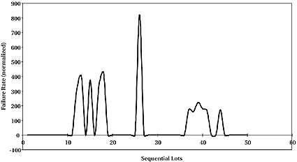
Figure 1 shows the normalized percent failure from a particular semiconductor process measured on the first 50 production lots subjected to a sample burn-in program. Analysis of the failures seen in this study identified three separate process issues. Correction of these issues eventually led to more stable reliability. None of the issues was detected in the initial three-lot qualification program.
Infant Mortality
There are generally three distinct areas of analysis in semiconductor reliability. The first area is the "infant mortality" section of the "reliability bathtub curve" (Figure 2). Device failures due to built-in defects, such as particle defects, etch defects, scratches, and package assembly defects, dominate this region of the lifetime curve. These are the most common defects identified by burn-in tests and typically correlate with wafer functional yield [1].
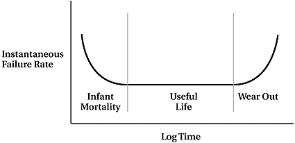
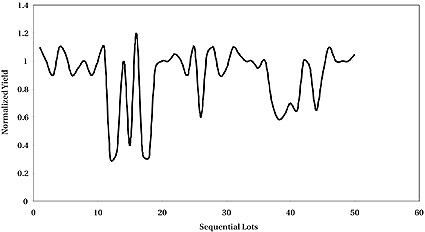
Figure 3 illustrates the correlation between low yield and sample burn-in fallout for the 50 burn-in lots of Figure 1. The strong correlation suggests that wafers or lots with anomalous low yield will show a significantly higher risk of reliability fallout. Therefore, the first step in a reliability process control program is to use the yield data generated during functional die testing at the wafer level as a measure of defect density. Wafers, or entire wafer lots, that have a statistically different yield should be identified as anomalous material and subjected to engineering analysis, burn-in, or simply scrapped.
A short high voltage stress is another common way of obtaining a quick measure of the infant mortality defect density. Such stress increases the electric field across the gate oxide and increases current density in interconnect lines. This one to three second test can identify nearly open metal lines and "thin" oxides.
An IDDQ test [2] for CMOS products can significantly increase sensitivity to oxide defects. This test measures the quiescent current of the product and reveals an increase in the gate oxide leakage.
The steps to perform this measurement are:
- Measure the IDDQ current for several test vectors.
- Force a high voltage stress (e.g. 4V for a 3.3V process) for three seconds.
- Measure the IDDQ current again for the same test vectors.
- Calculate the change in IDDQ current.
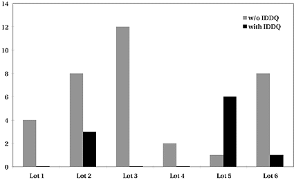
Once again, the number of defective devices is an initial measure of infant mortality. Wafers or lots that show a higher than normal fallout on this stress test can be considered anomalous material. Figure 4 compares burn-in fallout from six split lots. Half of the lots were subjected to the stress/IDDQ test, while the other half were not. With the exception of Lot #5, the stress/IDDQ stress identified most of the burn-in fallout.
Wearout Failures
The last section of the reliability bathtub curve shows an increasing failure rate. There are no anomalous "defects" in material that fails in this section of the reliability curve: the parts are "perfect." Wearout failures are caused by mechanisms such as electromigration, time dependent dielectric breakdown, and hot carrier degradation.
Mechanism-specific high stress tests are typically used to measure a "time to wearout". Burn-in tests or operational life tests are not particularly useful because the stress conditions cannot normally be accelerated enough to create failures in good material within a reasonable time (e.g., 2000 hours).
Fast WLR Testing
Fast WLR tests can reduce the time and expense of measuring reliability variations due to wearout mechanisms. A typical suite of Fast WLR tests takes about 90 seconds and is performed on specific test structures designed into the scribe lanes of the wafer. Each structure is designed to test for only one potential failure mechanism that correlates with degradation.
Fast WLR tests are not meant to determine a projected lifetime under use conditions. Drawing conclusions about a ten-year lifetime based on the results of a given three-second test is inadvisable. Such a projection would require extrapolation over eight decades in time (most reliability failures are linear in the log time domain). A three-second measurement typically provides data over only three, or in a best-case scenario, six time decades.
On the other hand, numerous papers [
The longer traditional tests determine whether tested material meets the reliability level required by the intended application. If it does, then Fast WLR testing provides a statistical distribution of the material's performance. All subsequent material can be compared to this statistical benchmark. If there is no statistical difference in the performance of subsequent material, then engineers can conclude that subsequent material will have the same reliability as the qualification material. Otherwise the subsequent lot is anomalous material needing further engineering study.
The goal of this approach is to reduce process variation, not to prove that the material is better than some minimum acceptable level. Due to interaction effects within a complex semiconductor process, more process variation tends to increases the probability of reduced reliability in some future product lot. The number of potential interaction effects in a modern semiconductor process is nearly infinite. Simply identifying a single cause of failed material will never produce the information needed to reduce the failure rate of future material.
Cost and Time Savings
Time and test cost savings can be substantial. As noted previously, identifying process reliability variations using traditional test techniques would require more than 200 days, destructive testing of 7,500 product die, and test equipment capable of testing 2,500 devices in parallel. Reliability process control testing can be accomplished on the same day as the material becomes available, using test equipment capable of testing only one die at a time. The yield is normally measured on every wafer as part of the normal production process, but no product is consumed. Further, the Fast WLR tests can generally be combined with the normal parametric tests and typical test times are on the order of 90 seconds per site for 30 different tests.
These cost savings are achieved only as long as the tested material is statistically identical to the baseline material. If material is found to be dissimilar, then traditional reliability test techniques are required to quantify the difference.
About the Author
Keithley Instruments, Inc.
References
The goal of process reliability control testing is to reduce variation in the reliability of a semiconductor process. This approach to testing is the most efficient program for driving reliability improvement. It uses the initial product yield analysis and Fast WLR test techniques to reduce the time and cost required to monitor or qualify a process change or new fab line. Once a statistical baseline is established, short process control tests are sufficient to prove that the new fabrication process or line produces statistically similar product.
Timothy Turner is Director of Structures Engineering in Keithley's Semiconductor Division where he is responsible for design and development of wafer test structures and device reliability algorithms, which are part of Keithley's Wafer Level Reliability (WLR) product line. He previously owned and operated Turner Engineering, specializing in accelerated test methods that allow reduced time to market, high stable yields, and assured reliability for semiconductor fabs. His 20 years of experience in semiconductor reliability includes organizations such as the Reliability Analysis Center in Rome, NY and Mostek Corporation in Carrollton, TX. He has been issued six US patents in the field of semiconductor processing, and has published more than 25 papers in the field of semiconductor reliability and processing.
28775 Aurora Road
Cleveland, Ohio 44139
Phone:+1 440-248-0400
Fax: +1 440-248-6168
[1] F. Kuper et. al., "Relation Between Yield and Reliability of Integrated Circuits: Experimental Results and Application to Continuous Early Failure Rate Reduction Programs," in Proc. 1996 IRPS, 1996, pp. 17-21.
[2] B. Root and T. Turner, "Wafer Level Electromigration Tests for Production Monitoring," in Proc. 1985 IRPS, 1985, pp. 100-108.
[3] T. Turner, "Consistency of Similarly Designed Wafer Level Reliability Test Structures Produced in Multiple Fabrication Areas," in Final Report: 1992 Intl Wafer Level Reliability Workshop, 1992, pp. 215-219.
[4] S. Foley et. al., "Evaluation of Test Methods and Associated Test Structures for Interconnect Reliability Control," in Proc. 1999 Intl Conf. on Microelectronic Test Structures, 1999, pp. 167-172.
[5] J. Sweet and D. Peterson, "High Accuracy Die Mechanical Stress Measure-ment with the ATC04 Assembly Test Chip," Final Report: 1993 Integrated Reliability Workshop, pp. 90-97.
[6] B. Aldridge, et. al., "Detection and Measurement of Hot Carrier Degradation Associated with Asymmetric P-Channel Transistors," Final Report: 1995 Integrated Reliability Workshop, pp. 66-71.
[7] L. Anderson, et. al., "A Case Study in a 100 Reduction in Sodium Ions in a 0.8m BiCMOS Process using Triangular Voltage Sweep," Final Report: 1995 Integrated Reliability Workshop, pp. 45-48.
[8] G. Madson, et. al., "Building Reliability into an EPROM Cell Using In-Line WLR Monitors," Final Report: 1995 Integrated Reliability Workshop, pp. 40-44.
[9] D. Bang, et. al. "Effect of Cu Damascene Metallization on Gate SiO2 Plasma Damage," 1993 3rd International Symposium on Plasma Process-Induced Damage, pp. 64-65 (IEEE cat.#: 98EX100).
[10] W. Lukaszek, "EEPROM-based Charging-Effects Sensors for Plasma Etching and Ion Implantation" Final Report: 1992 International Wafer Level Reliability Workshop, pp. 101-105.
[11] R. Gestel, Reliability Related Research on Plastic IC-Packages: A Test Chip Approach, Delft University Press, Geboren te Breda, Netherlands, 1994.